Impedances. You come across this property in various technical fields. Some examples are acoustics, optics, electrical circuits, to name a few.
Impedance is what the word says: the act to impede something. In case of wave propagation, this would be to impede propagation. This happens when a wave travels from one medium to another. In the case of an electrical circuit, impedance is the act to hinder a current in a circuit.
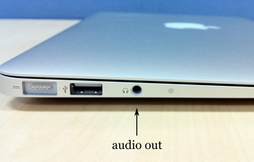
In this blog I will go a bit into this electrical impedance. And to be specific, impedances when connecting to circuits or devices. You deal with this whenever you electrically connect some output to an input. You can think of connecting your set of headphones to an amplifier or an audio-output of your notebook. But also for cable-tv when you are connecting the coaxial cable to the television set. Other, more technical, examples would be measuring voltages using an oscilloscope or simply connecting a sensor to a circuit.
In all these example it comes down to electrically connecting one thing to the other. We then deal with output and input circuits. Each of them have their own impedance. So what is the relation between them?

To understand input and output impedances we use Thevenin’s equivalent circuit for the output. This means we can simplify any circuit as a voltage source and a resistor in series.
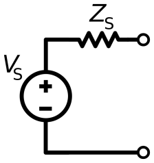
Here 

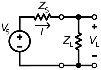
This circuit now delivers power to the electrical load 
Using Ohm’s law 
.

We can see that the circuit is simply a voltage divider. The voltage load can be 

Now let’s look at the power 
For the total power we get
,
which give its absolute maximum power when the load is zero,

.
The power over the load is
.
We can now determine for which load impedance 
.
For the derivative we get 
Now this equals zero for the load 
.
Which means we have maximum power transfer when the load equals the source impedance. We also call this impedance matching. Now let’s take a look at the power of the load 


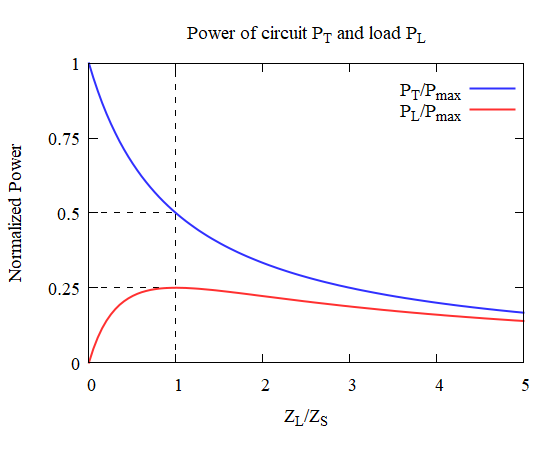
The blue line tells us, as expected, that the total power of the system decreases as the load increases. The red line shows us that indeed there is a maximum of power transfer over the load when 
If we look away from this point we see that for lower values 

For larger load impedances 
Usually having the load voltage to be equal to the source voltage (i.e. when 
We can summarize the load impedance cases as follows:
This is what we want to prevent. Having too low load impedance can cause damage to the circuit.
Also called impedance matching. This conditions ensures maximum power transfer. You can see this as the lower limit you want for the load impedance.
Also called impedance bridging. The power over the load is not at a maximum, but the total circuit is generally considered safe and works properly.
The last bullet point is what is desired for audio systems, such as headphones. In a next blog I will discuss how to apply the knowledge of in- and output impedances given in this blog to speakers, headphones, amplifiers and other output devices.
Extension to AC circuits:
As a last point I want to make a short comment about the extension to AC circuits. Now we have only talked about the case when the impedance is purely resistive which is a very simplified case. In practice, and especially in audio applications, the impedance is actually complex and depends on the frequency of the signal. While manufacturers may give a single number for the impedance for an input device, the value changes depending on the frequency of the signal coming out of the output. It is possible you can get a curve of the impedance vs the frequency from the manufacturer. Usually there is some resonant frequency for which the impedance peaks.
Because of the coils inside the headphones (which move a membrane using a coil and a magnet with the purpose to generate the acoustic waves as variations in pressure density to generate the sound we hear) we can expect this to behave as an inductor. So in reality the impedance will indeed be complex. In practice this means that the signal coming from the output circuit will be somehow shifted in phase when arrive at the vibrating membrane. This is not a concern when using your headphones. It can become a concern when this (additional) phase shift is not linear in frequency and start to distort the sound. But this is all another topic. 🙂
